Professionals
Trained
Accelerate your entry into the semiconductor industry with specialised VLSI training and practical exposure.
 Understand the Roles
  Compare Career Paths
  Identify the Right Direction



Backed by Faculty Averaging 15+ Years of Industry Experience
 Hyderabad
Professionals
Trained

Placement
Offers Secured

Highest Package
Achieved

Hiring
Partners
Driving core technological advancement across modern electronic systems.
S.I.T. offers specialised courses in Design Verification, Physical Design and Analog Layout - each structured to build the knowledge, workflows and practical capability required for its corresponding career path.
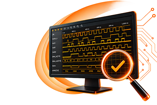
Find Design Errors Before Fabrication
Verify functional behaviour and confirm that a digital design performs as intended.

Turn Digital Logic into a Manufacturable Chip
Build the physical implementation while balancing performance, power and area.

Translate Circuit Intent into Precise Layout
Create analog circuit layouts, accounting for matching, performance and design constraints.

Learn with faculty averaging 15+ years of experience in the semiconductor industry.

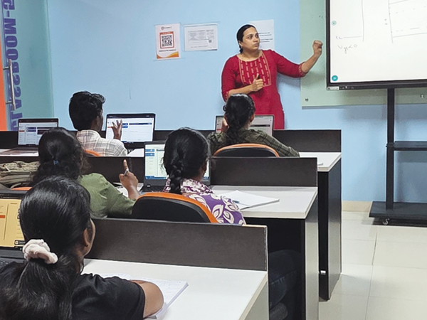
Benefit from greater faculty interaction, focused guidance & more opportunities to clarify concepts.

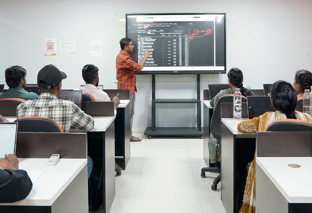
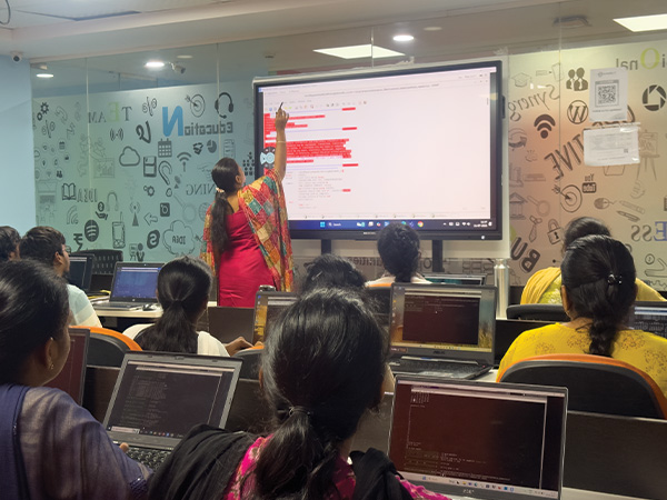
Build practical familiarity with industry-relevant EDA tools in a structured lab environment.

Investigate, analyse, implement and validate across realistic design situations.

Use S.I.T.’s AI-powered solution for debugging, analysis, automation and problem-solving.

Extend technical training through structured practical and industry exposure.
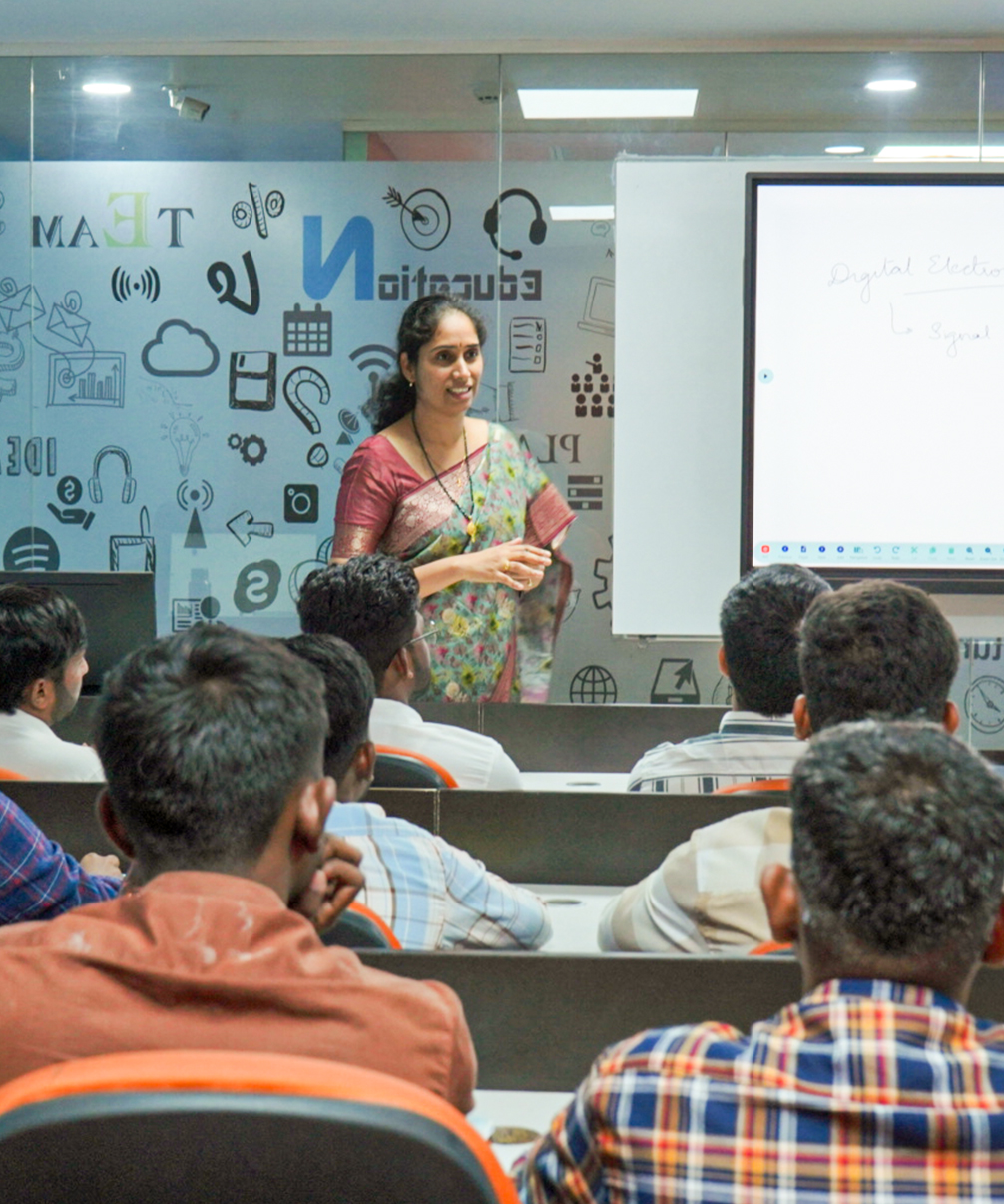

S.I.T. was established to help engineering graduates move from broad academic foundations towards defined careers in the semiconductor industry. Our purpose is to provide the direction, technical capability and practical exposure required to pursue specialised VLSI roles with confidence.
Identify relevant VLSI roles and opportunities aligned with the selected specialisation.
Strengthen practical readiness through guided tool practice and project work in dedicated labs.
Present technical skills, projects, tools, and internship experience through a role-focused resume.
Prepare for technical assessments, role-specific discussions and mock interviews.
Access relevant openings through S.I.T.’s network of hiring partners.
Hear directly from our alumni about choosing a specialisation, building practical capability and progressing into semiconductor roles.
The Physical Design training helped me understand industry workflows beyond academic theory, with faculty who explained how concepts are applied in engineering teams.

Hands-on lab sessions and structured assignments made Design Verification much clearer, and the internship exposure connected classroom learning with real project work.

Domain-focused Analog Layout training and internship exposure helped me prepare for semiconductor design roles with practical confidence.













S.I.T. prepares learners for specialised roles in Design Verification, Physical Design and Analog Layout.
Design Verification validates functional behaviour, Physical Design converts digital logic into physical implementation, and Analog Layout translates circuit intent into precise layouts.
Electronics and Communication Engineering, Electrical and Electronics Engineering, Electronics, Instrumentation and related engineering disciplines may be eligible. Suitability varies by specialisation.
The choice depends on technical interests, academic foundations and preferred type of engineering work. S.I.T. counsellors can help compare the roles.
Prior experience may not be required. Course-specific eligibility and prerequisites should be confirmed before enrolment.
Yes. Training includes EDA tool application, design scenarios, lab practice and a structured six-month internship.
S.I.T. supports résumé development, technical preparation, mock interviews and access to relevant hiring opportunities. Placement outcomes depend on eligibility, performance and available roles.
Speak with our career counsellor to understand role suitability, course options, eligibility and the admission process.
JNTU Metro Station, Fortune Signature Towers, Nizampet X Roads, Hyderabad 500085